P8: 4-bit shift register
2026-03-11T23:59
Goals
- Demonstrate your knowledge of sequential circuits
Objective
For this problem, you will implement a 4-bit shift register. A shift register can be used like a normal register – values can be loaded in and then they are stored until we change them. The shift register adds one wrinkle, in addition to loading in new values, it can also perform a shift in which the values of all of the bits move over one to their neighbor.
There are left-shift and right-shift registers. While there are a number of reasons we might want to shift the bits in a register, one of the more important reasons is that it is a quick way to multiply by 2 (left shift) or divide by 2 (right shift).
I would like you to implement a right shift register
Requirements
- your work must be in a file called
shift_register.circ - your implementation must be in the
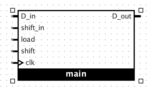
maincircuit (you are welcome to create sub-circuits however) - your circuit must have four inputs:
D_in,load,shift,shift_inand theclk D_inwill be a 4-bit valueshift_inis a 1-bit valueloadandshiftare 1-bit inputs.- When
loadis 1 andshiftis 0. The register should loadD_ininto the register on the next clock edge - When
storeis 1 andloadis 0, the register should perform a right shift on the next clock edge. The value ofshift_inwill be shifted into the most significant bit. - If both
loadandshiftare 1, the behavior is undefined (i.e., you can ignore this) - The circuit has one output
D_out - At all times,
D_outshould reflect the value currently stored in the register - you are restricted to
- input pins
- output pins
- splitters
- components in the Gates library (i.e., basic logic gates)
- components in the Plexers library
- D flip flops
Testing sequential circuits is less straightforward than using the test vectors we could use for combinational circuits. I basically have a test harness that I plug your circuit into. This means that your pin arrangement needs to match mine.
Right side:
D_inshift_inloadshift
Left side:
D_out
If you haven’t started yet, here is a starter circuit (be sure to rename the file).
Submission
Upload your .circ file to Gradescope.